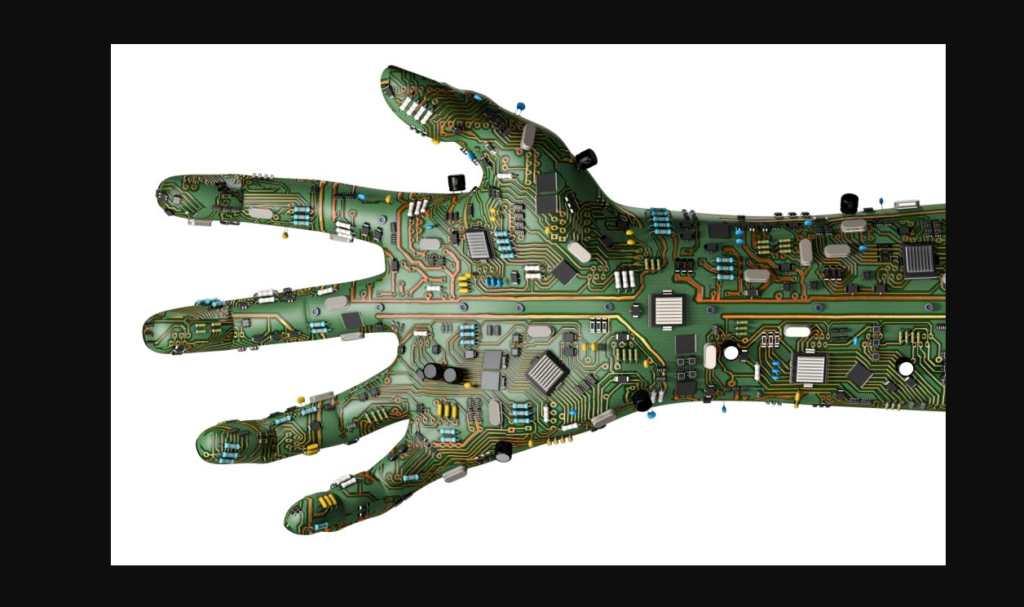
Printed Circuit Board (PCB) design refers to the method of creating a layout for digital circuits used in diverse devices. The team employs a systematic technique to create a layout that includes the electrical components and their connections, ensuring the design is optimized for performance, manufacturability, and cost. eTAZ systems PCB layout is one of the most crucial phases in electronics production, because it guarantees the functionality, reliability, and durability of the product while it’s miles entire.
During the layout manner, several steps ought to be accompanied, including schematic seize, factor placement, routing, and verification. We cautiously control these steps to ensure that the final board operates precisely as intended. With the fast advancement in generation, PCB designs have grow to be increasingly state-of-the-art, and today’s designs need to fulfill stringent performance criteria, specifically in highly specialised fields like telecommunications, automobile, and aerospace industries.
Steps in the PCB Design Process
Schematic Capture: In this first step of the PCB layout process, you create a visual representation of the digital circuit. The schematic is an in depth drawing showing how all the components are related. It is sort of a blueprint for the circuit, permitting designers to visualise how the complete gadget will work before moving ahead.
Component Placement: Once the schematic is ready, the following step is to area the components on the board. Proper placement is essential as it affects how well the board features, its size, and its manufacturability. Designers should make sure that additives are located to reduce interference, reduce sign delays, and maximize performance.
Routing: This section involves connecting the numerous additives placed at the board thru electric paths referred to as traces.Ensure that all components are well connected and that the traces do not cause any interference or signal degradation during routing. It is crucial to preserve clearances and keep away from overcrowding.
Verification: Once the layout is whole, it is going via a verification procedure to make sure it meets all the design necessities. This consists of walking simulations and tests to test for capability troubles like short circuits, signal delays, and mistaken connections. Correct any mistakes or design flaws before the board goes into manufacturing.
Types of PCB Designs
Single-Layer PCBs: These are the most primary kind of PCBs and encompass best one layer of conductive fabric. They are generally utilized in simple gadgets like calculators and power supplies. Single-layer PCBs are smooth to layout and manufacture, making them price-powerful for easy applications.
Double-Layer PCBs: Double-layer PCBs have layers of conductive cloth, making an allowance for more complex circuit designs. These are widely used in purchaser electronics like smartphones, drugs, and different hand held devices. The additional layer affords greater routing alternatives and increases the overall overall performance of the board.
Multi-Layer PCBs: Multi-layer PCBs include three or more layers of conductive fabric, making them suitable for extra sophisticated packages. These are generally used in high-overall performance devices like scientific system, aerospace structures, and advanced verbal exchange structures. Multi-layer PCBs offer higher overall performance, higher capacity, and more reliability.
The maximum commonplace kind of PCB is used in numerous applications, from household appliances to business machines. They provide a sturdy and durable platform for components and manufacturers typically use them in long-lasting devices.
Flexible PCBs, also known as flex circuits, designers create to be flexible, allowing users to bend or fold them to fit into tight spaces. Designers commonly use these in applications where space is a constraint, such as wearables, medical devices, and compact electronics.
Rigid-flex PCBs combine rigid and flexible designs, enabling engineers to create complex applications that require both flexibility and rigidity. Manufacturers typically use these in military, aerospace, and medical devices, where reliability and performance are vital.
Importance of PCB Design in Electronics
Functionality: A nicely-designed PCB is crucial to make certain that the electronic device features well. Poor design can result in malfunctioning, improved electricity intake, and heat era.
Reliability: PCB layout performs a essential position in figuring out the reliability of the device. A properly-designed board will make certain that the product features effectively for its meant lifespan, with out frequent breakdowns or repairs.
Cost Efficiency: Optimizing the PCB layout can reduce production fees via minimizing the wide variety of components used, decreasing board size, and enhancing the manufacturability of the design.
Durability: The layout of a PCB at once affects the durability of the very last product. A strong PCB design ensures that the product can withstand environmental strain, mechanical shock, and thermal biking, enhancing the general durability.
PCB Design Tools and Software
Designing a PCB calls for the usage of specialised software program tools which can create, simulate, and take a look at the format. Some of the most famous PCB layout equipment include:
Altium Designer: One of the maximum broadly used PCB design tools, Altium Designer offers a comprehensive suite of features, along with schematic capture, PCB format, and simulation. Many people consider it for its consumer-friendly interface and effective layout capabilities.
KiCad: KiCad is an open-source PCB design tool that offers a complete suite of layout capabilities, which include schematic capture, PCB format, and 3D visualization. It is famous amongst hobbyists and small-scale manufacturers.
OrCAD: OrCAD is a effective PCB layout device used in professional settings. It offers advanced capabilities like layout rule checking, sign integrity analysis, and automatic routing, making it suitable for complex designs.
Challenges in PCB Design
Signal Integrity: Maintaining signal integrity presents one of the most important challenges in PCB design, especially in high-pace applications.. Designers must make certain that alerts journey with out distortion or loss, which may be difficult to attain in complex layouts.
Thermal Management: Heat dissipation is some other foremost assignment in PCB design. As electronic components generate warmth, it’s miles essential to design the board in a manner that ensures proper warmness management, preventing additives from overheating.
Component Placement: Ensuring most appropriate placement of components at the PCB is a sensitive balancing act. Designers must bear in mind electrical performance, manufacturability, and area constraints, which can be tough to achieve concurrently.
Design for Manufacturability (DFM): A PCB ought to be designed with production in mind. Complex designs which can be tough to fabricate can lead to higher charges and longer production times. Designers have to make sure that the layout can be easily produced the usage of available production techniques.
FAQs on PCB Design
What is the main reason of PCB layout?
The number one reason of PCB layout is to create a functional and reliable format for digital circuits, ensuring that the device operates efficaciously and price-effectively.
How long does the PCB design method take?
The time required for PCB design can range depending at the complexity of the circuit. Simple designs can also take some days, even as greater complicated designs can take numerous weeks.
Can we automate PCB design?
While automation can handle some elements of PCB layout, such as routing and simulation, humans must ensure the best design and performance through their understanding.
What factors should designers take into consideration when designing a PCB?
Consider factors like sign integrity, component placement, thermal control, and manufacturability throughout the PCB design process.
What is the distinction among single-layer and multi-layer PCBs?
Single-layer PCBs have simplest one conductive layer, making them suitable for easy packages, at the same time as multi-layer PCBs have more than one layers, allowing more complicated designs and higher performance.
Additionally ETAZ Systems is at the forefront of imparting brand new PCB design offerings. With understanding in growing robust and efficient PCBs, they provide tailored solutions for a wide variety of industries, making sure that each layout meets the best requirements of pleasant and reliability. Whether you are working on a simple tool or a high-performance application, eTAZ Systems delivers cutting-edge PCB designs that power tomorrow’s technology.