
The motherboard, regularly taken into consideration the backbone of a pc, performs a crucial position in making sure all components work harmoniously. Its design, in particular the Printed Circuit Board (PCB), is a complex and complex process that demands precision, know-how, and meticulous attention to element. eTAZ systems This article delves into the necessities of motherboard PCB layout, highlighting key steps, excellent practices, and commonplace FAQs.
Understanding Motherboard PCB Design
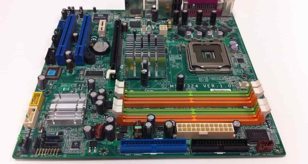
1. PCB Layers and Materials: Motherboards are commonly multi-layered PCBs, with every layer serving a specific motive, which include sign routing, power distribution, or grounding. Common materials used consist of FR-four epoxy laminate, recognised for its excellent mechanical and electrical properties.
2. Schematic Design: The design procedure starts offevolved with a schematic, a blueprint that outlines the electrical connections among additives. This step includes selecting components, defining connections, and making sure all elements are like minded.
3. Component Placement: Strategically placing components on the PCB is vital for top-quality overall performance. Key issues consist of signal integrity, thermal control, and minimizing electromagnetic interference (EMI).
Four. Routing: Routing entails developing pathways for electrical indicators to journey among additives. This step calls for cautious planning to avoid signal degradation, crosstalk, and other troubles that might compromise the motherboard’s overall performance.
Five. Power and Ground Planes: Proper distribution of electricity and grounding is important for balance. Power planes offer a uniform voltage to additives, at the same time as ground planes function a reference point and assist lessen noise.
6. Thermal Management: Effective thermal control ensures that components perform within secure temperature tiers. This can involve including heat sinks, thermal vias, and proper spacing to facilitate heat dissipation.
7. Testing and Validation: Once the design is complete, rigorous testing is conducted to become aware of and rectify any troubles. This consists of signal integrity testing, electricity analysis, and thermal simulation.
FAQs on Motherboard PCB Design
Q1: What software program is commonly used for motherboard PCB design?
A: Popular PCB layout software consists of Altium Designer, Eagle, KiCAD, and Cadence Allegro. These tools offer capabilities for schematic seize, layout design, and simulation.
Q2: How many layers are typically in a motherboard PCB?
A: Motherboards frequently have among 6 to twelve layers, depending at the complexity and necessities of the design. High-quit motherboards may additionally have even extra layers to deal with superior capabilities.
Q3: What are differential pairs, and why are they essential?
A: Differential pairs are lines that carry identical and opposite signals. They are important for excessive-speed records transmission as they reduce noise and improve signal integrity.
Q4: How do you manage thermal troubles in motherboard layout?
A: Thermal control includes the usage of warmness sinks, thermal vias, adequate spacing between additives, and making sure proper airflow inside the enclosure.
Q5: What is the function of decoupling capacitors in PCB design?
A: Decoupling capacitors filter out noise from the strength supply, making sure a strong voltage deliver to the additives. They are placed near strength pins of integrated circuits.
Q6: How can EMI be decreased in motherboard layout?
A: Reducing EMI entails the usage of ground planes, protective sensitive components, preserving proper spacing among strains, and the use of ferrite beads or chokes.
Q7: What are the common challenges in motherboard PCB design?
A: Common demanding situations consist of dealing with sign integrity, thermal troubles, power distribution, EMI, and making sure the design meets manufacturing constraints.
Q8: Why is trying out and validation essential in PCB layout?
A: Testing and validation are critical to discover and rectify ability problems earlier than mass production. This ensures the motherboard plays reliably and meets all specifications.
Conclusion
Designing a motherboard PCB is a complex assignment that calls for a deep knowledge of electronics, meticulous planning, and interest to element. By following first-class practices and addressing common challenges, designers can create sturdy, excessive-performance motherboards that electricity contemporary computing devices. Whether you’re a pro engineer or a newbie in PCB layout, expertise these ideas is important for achievement on this ever-evolving discipline.