Printed Circuit Boards (PCBs) are essential in modern electronics, acting as the critical foundation that connects and supports electronic components. At eTAZ Systems, we excel in creating advanced PCB designs to ensure your devices perform reliably and efficiently. This guide will walk you through the intricacies of PCB design, highlight our expertise, and answer some common questions.
What is PCB Design?
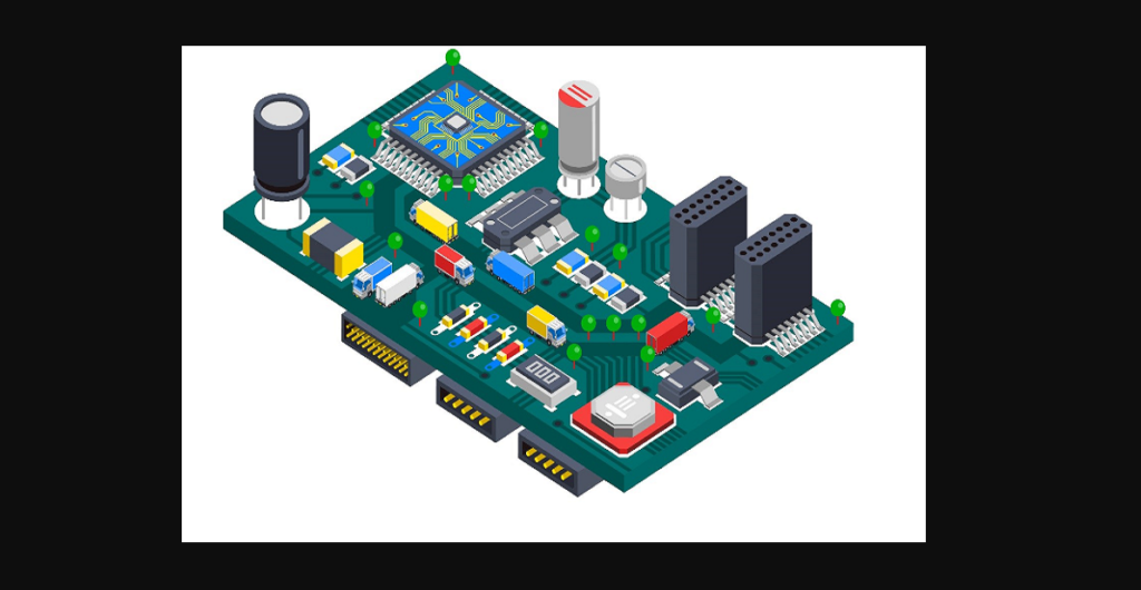
PCB design involves crafting the layout and schematics for a printed circuit board. A PCB provides both physical support and electrical connections for electronic components. The design process includes several steps: creating the schematic, laying out the PCB, routing connections, and preparing for manufacturing.
Why PCB Design Matters
- Reliability: A well-designed PCB ensures secure connections, which reduces the likelihood of failures and extends the product’s lifespan.
- Performance: Effective PCB design enhances signal integrity and power distribution, which is crucial for high-speed and high-frequency applications.
- Cost-Efficiency: A well-thought-out design minimizes material waste and manufacturing costs by optimizing layout and component placement.
Our PCB Design Services at eTAZ Systems
At eTAZ Systems, we offer a full suite of PCB design services tailored to various industries and applications. Our process is thorough and structured, from the initial idea to the final product.
- Schematic Capture: We start by creating a detailed electrical schematic that defines how components connect.
- PCB Layout Design: Our team carefully arranges components and designs the traces that connect them, ensuring the layout meets all specifications.
- Signal Integrity Analysis: We simulate and enhance the PCB’s signal integrity to tackle issues like crosstalk and electromagnetic interference.
- Thermal Management: We design cooling solutions to manage heat dissipation, crucial for maintaining performance and reliability.
- Design for Manufacturing (DFM): Our designs are optimized to be produced efficiently and cost-effectively.
- Prototyping and Testing: Before full production, we build prototypes and conduct rigorous testing to validate the design.
Key Considerations in PCB Design
- Component Placement: Strategically placing components minimizes interference and optimizes connection routing.
- Trace Routing: Proper routing is essential for maintaining signal integrity and avoiding electrical noise.
- Layer Stackup: The number of layers affects PCB complexity and performance. We design stackups to meet project requirements.
- Power Distribution: Ensuring proper power distribution and grounding is vital for stable operation.
- Design Rules and Constraints: We follow industry standards to ensure compatibility and reliability.
Why Choose eTAZ Systems?
- Expertise: Our team has extensive experience in designing PCBs for a range of applications, from consumer electronics to industrial systems.
- Advanced Tools: We use the latest design tools and software to create precise PCB layouts.
- Quality Assurance: We follow strict quality control procedures to ensure each PCB meets high standards.
- Custom Solutions: We provide tailored PCB design solutions to fit your specific needs.
FAQs
What’s the typical turnaround time for PCB design at eTAZ Systems?
Turnaround time varies based on project complexity, usually ranging from 2 to 6 weeks. We provide detailed timelines tailored to your needs.
How do you ensure the quality of your PCB designs?
We ensure quality through rigorous design reviews, simulations, and testing. Our designs go through multiple verification stages to address potential issues.
Can you handle both small and large-scale PCB manufacturing?
Yes, we manage both small prototypes and large-scale manufacturing runs, adapting to projects of different sizes and complexities.
What industries do you serve with your PCB design services?
We work with various industries, including consumer electronics, automotive, medical devices, telecommunications, and industrial automation.
Do you offer support for PCB assembly?
Yes, we handle PCB assembly, including component sourcing, soldering, and final testing, ensuring a smooth transition from designs to finished product.
What types of PCBs do you design?
We design single-layer, double-layer, and multi-layer boards, catering to both simple circuits and complex high-density interconnects.
How do you handle design changes or revisions during the project?
We accommodate changes based on your feedback and work closely with you to incorporate modifications while adhering to timelines and budgets.
What is the cost of PCB designs services at eTAZ Systems?
Costs depend on factors like complexity, size, and specific requirements. We provide customized quotes based on your project details.
Can you assist with PCB design for IoT applications?
Absolutely. We have extensive experience designing PCBs for IoT applications, including those with wireless communication and advanced sensing.
How do you handle confidential or proprietary designs?
We prioritize confidentiality with strict measures to protect your designs, including non-disclosure agreements (NDAs) and secure data handling practices.
Conclusion
PCB design is a crucial aspect of electronics engineering. At eTAZ Systems, we are committed to providing high-quality, reliable, and efficient PCB solutions. Whether you’re developing a prototype or scaling up to production, eTAZ Systems is your trusted partner for PCB designs.
For more information or to discuss your PCB designs needs, contact us at eTAZ Systems today.