Printed Circuit Boards (PCBs) are the spine of contemporary digital gadgets, supplying the bodily structure to help and connect digital additives. However, you must design a detailed schematic before creating a PCB eTAZ systems.
Additionally schematic serves as a blueprint and shows how everything interconnects.
Transitioning from a PCB design again to a schematic can be tough but essential for troubleshooting, opposite engineering, or documentation functions. Moreover This article explores the procedure of changing a PCB layout to a schematic and addresses a few not unusual questions on the system.
Understanding the Basics

What is a PCB?
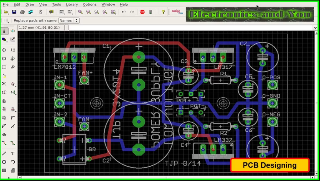
A Printed Circuit Board (PCB) connects and aids digital components using conductive pathways, tracks, or signal lines etched from copper sheets laminated onto a non-conductive substrate.
What is a Schematic?
A schematic diagram also graphically represents an electrical circuit, showing how special additives connect using symbols and lines.”
The Importance of Converting PCB to Schematic
Reverse Engineering: Understanding how an existing PCB works when documentation is unavailable.
Troubleshooting: equally Identifying and diagnosing troubles in an existing circuit.
Documentation: Creating a reference for future repairs, modifications, or educational purposes.
Frequently Asked Questions (FAQs)
Q1: Why would I need to convert a PCB returned to a schematic?
A1: Converting a PCB to a schematic is regularly necessary for reverse engineering, troubleshooting, and creating documentation for maintenance or modifications. It enables in expertise the functionality and layout of an present PCB.
Q2: What tools are required for changing PCB to schematic?
A2: Essential gear include a multimeter or continuity tester for tracing connections, schematic seize software for drawing the schematic, and possibly a magnifying glass or microscope for examining small additives.
Q3: Can software program automate the PCB to schematic conversion manner?
A3: While a few advanced software program tools can assist in identifying connections and components, complete automation is difficult due to the complexity and variability of PCBs. Manual verification is often required.
Q4: How can I identify unmarked or difficult to understand additives on a PCB?
“Sometimes, you can recognize unmarked components by using their circuit function, datasheets, or by comparing them with similar known circuits. Online boards and communities also can be helpful assets for identifying obscure additives.
Q5: What are not unusual mistakes to avoid all through the conversion system?
A5: Common errors include lacking connections, incorrect aspect values, and misinterpretation of multi-layer PCB connections. Careful documentation and verification at every step can help keep away from these mistakes.
Conclusion
Engineers involved in reverse engineering, troubleshooting, and documenting digital circuits must master the ability to convert a PCB to a schematic. Despite the demanding situations, with the proper approach and tools, it may provide valuable insights into the layout and functionality of digital gadgets. Whether for repairing an vintage circuit or knowledge a complex layout, learning this manner is an invaluable asset inside the area of electronics engineering.
Contact Us.
For more facts approximately our PCB to Schematic Simulation services or to speak about your challenge necessities, please attain out to us at:
Office: #9, First floor, Business Incubation Center SSC, Therefore University of Engineering and Technology, Lahore.
Phone: +923234767694
Email: info@etazsystems.Com
At eTAZ Systems, we are then devoted to handing over exceptional PCB design answers that meet your precise desires and help you obtain your assignment goals.