Printed Circuit Board (PCB) layout is a essential component of modern electronics. From easy gadgets to complex machinery, eTAZ systems PCBs are the spine that connects and helps electronic additives
Importance of PCB Design
PCB layout is essential for numerous motives
Component Organization: Proper PCB design guarantees that each one additives are nicely-prepared and positioned optimally to function successfully.
Electrical Pathways: It presents reliable electric connections and pathways for present day to waft among components.
Size Reduction: Besides Modern PCBs permit for the miniaturization of electronic gadgets, making them compact and portable.
Durability: High-nice PCB layout enhances the sturdiness and toughness of electronic devices.
Cost Efficiency: Efficient PCB layout can lessen production expenses and enhance the overall overall performance of the product.
Printed Circuit Board (PCB) Design FAQs: Everything You Need to Know
Printed Circuit Boards, normally called PCBs, Similarly are important components in almost all electronic gadgets we use nowadays. From smartphones to industrial equipment, nevertheless PCBs play a critical position in offering connectivity and capability to those devices. Designing a PCB is a complex and intricate system that calls for careful planning and execution. In this article, we can deal with some frequently asked questions concerning PCB layout.
1. What is a Printed Circuit Board (PCB)?
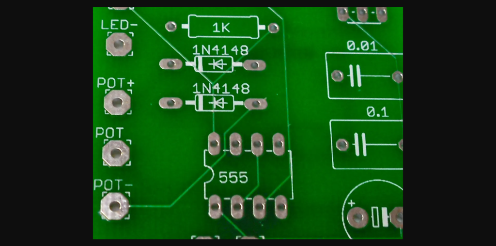
Manufacturers make a Printed Circuit Board from non-conductive material, usually fiberglass, and set up digital components on it, connecting them using conductive lines. Copper typically forms these traces, providing the electric pathways for the components to communicate with each other.
2. Why is PCB Design Important?
PCB layout is critical as it determines the functionality, equally reliability, and overall performance of an electronic tool. A nicely-designed PCB can reduce signal interference, enhance thermal management, and ensure the efficient operation of the device.
3. What are the Key Considerations in PCB Design?
When designing a PCB, elements together with factor placement, hint routing, sign integrity, thermal management, and manufacturability have to be taken into account. Therefore considerations help ensure the choicest overall performance and reliability of the final product.
4. What Software Tools are Used for PCB Design?
There are numerous software program tools available for PCB design, including Altium Designer, Eagle, KiCad, and OrCAD. These tools provide capabilities like schematic seize, overall PCB format, simulation, and design rule checking to resource designers in creating exquisite PCBs.
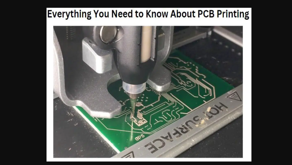
5. How are PCBs Manufactured?
The system known as PCB fabrication manufactures PCBs. This procedure includes numerous steps, which include designing the PCB format, creating the Gerber files, printing the circuit on the board, etching away the extra copper, drilling holes for components, and assembling the additives onto the board.
6. What are the Different Types of PCBs?
There are diverse forms of PCBs available, including single-layer, double-layer, and multi-layer PCBs. Engineers use single-layer PCBs in simpler applications, while they use multi-layer PCBs for complex designs that require multiple signal layers.
7. How Can I Ensure the Reliability of my PCB Design?
To make sure the reliability of your PCB design, it’s far essential to comply with first-rate practices including minimizing signal strains duration, supplying right grounding and energy distribution, the use of first-class components, and carrying out thorough checking out and validation.
8. What Are Some Common Mistakes to Avoid in PCB Design?
Some commonplace errors to avoid in PCB layout consist of inadequate thermal control, wrong sign routing, inadequate clearance between additives, overlooking design constraints, and neglecting to consider manufacturability problems.
9. How Can I Improve the Performance of my PCB Design?
To enhance the overall performance of your PCB layout, you may optimize sign routing, decrease sign reflections, lessen noise and interference, put into effect proper decoupling, and optimize energy distribution on the board.
In conclusion, PCB layout is a crucial factor of electronics layout that calls for interest to detail, knowledge of high-quality practices, and the usage of right gear. By addressing those FAQs and following industry standards, designers can create brilliant PCBs that meet the performance and reliability necessities of modern-day electronic devices.
Contact Us.
For extra statistics approximately our Printed Circuit Board (PCB) Design
offerings or to speak about your mission necessities, please reach out to us at:
Office: #9, First floor, Business Incubation Center SSC, University of Engineering and Technology, Lahore.
Phone: +923234767694
Email: data@etazsystems.Com
At eTAZ Systems, we deliver fantastic PCB layout solutions that meet your precise desires and help you achieve your task goals.