PCB Circuit Board Design (PCBs) are the spine of current digital gadgets. From easy gadgets to complicated machinery, PCBs facilitate the integration and capability of digital components. eTAZ systems This article delves into the essentials of PCB design, together with its significance, design method, and not unusual FAQs.
What is a PCB?
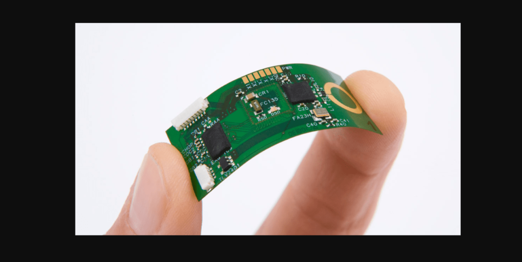
A Printed Circuit Board (PCB) helps and electrically joins digital components using conductive pathways, tracks, or signal traces etched from copper sheets laminated onto a non-conductive substrate.
Importance of PCB Design

Compact Size and Efficiency: PCBs permit for the compact arrangement of digital additives, decreasing the general size and improving performance.
Reliability: Properly designed PCBs make certain reliable performance via preserving steady connections and lowering the danger of short circuits.
Cost-Effective Production: Once the designers finalize a PCB layout, manufacturers will produce it cost-effectively and consistently.
Common FAQs approximately PCB Design
1. What software gear are typically used for PCB layout?
A: Popular PCB design software program consists of Altium Designer, Eagle, KiCad, OrCAD, and DipTrace. These equipment offer numerous functions for schematic capture, format design, and simulation.
2. What are the exclusive forms of PCBs?
A: There are several styles of PCBs, consisting of unmarried-sided, double-sided, and multi-layer PCBs. Manufacturers use special types like inflexible-flex PCBs and HDI (High-Density Interconnect) PCBs for particular programs.
3. How do I select the right PCB cloth?
A: The choice of PCB material relies upon on elements like sign velocity, running environment, and mechanical properties. Common substances encompass FR4 (fiberglass epoxy), PTFE (Teflon), and steel-middle PCBs.
4. What is the importance of PCB hint width and spacing?
A: Trace width and spacing affect the current-wearing potential and sign integrity. Wider strains can bring more current, while proper spacing prevents crosstalk and brief circuits.
5. How can I make sure signal integrity in my PCB layout?
A: To make sure sign integrity, preserve right hint impedance, decrease trace lengths, use differential pairs for excessive-speed alerts, and implement right grounding techniques.
6. What are a few not unusual PCB design mistakes to keep away from?
A: Common errors include inadequate spacing among strains, fallacious element placement, ignoring thermal control, and failing to carry out design rule exams (DRC).
7. How do I manage thermal issues in my PCB?
Answer: Thermal control strategies consist of using thermal vias, warmness sinks, and copper pours to deplete warmth. Proper element placement and adequate ventilation additionally assist control thermal problems.
8. What is a Gerber record?
A: A Gerber file is a wellknown record layout used to explain the PCB layout for production. It carries facts about the copper layers, solder mask, legend, and other PCB functions.
9. How can I lessen EMI (Electromagnetic Interference) in my PCB layout?
Answer: Reduce EMI by using the usage of proper grounding techniques, minimizing loop regions, protective touchy additives, and designing managed impedance lines for high-speed signals.
10. What are the stairs worried in PCB prototyping?
A: PCB prototyping involves creating a initial version of the PCB to check its functionality. Steps include design, fabrication, assembly, and trying out. Prototyping helps become aware of and clear up problems earlier than mass production.
Conclusion
PCB design is a important issue of electronic product improvement, requiring meticulous making plans and execution. Understanding the design method and addressing commonplace concerns ensures the advent of reliable and efficient PCBs. Whether you are a novice or an skilled dressmaker, non-stop mastering and adherence to high-quality practices will lead to successful PCB tasks.
By following this comprehensive manual and addressing the FAQs, you’re nicely-ready to embark for your PCB layout journey with self belief.
Contact Us
For greater statistics about our PCB Circuit Board Design or to speak about your unique assignment desires, please touch us:
Office Address: Office # 9, First floor, Business Incubation Center SSC, University of Engineering and Technology, Lahore.
Phone: +923234767694
Email: info@etazsystems.Com
At eTAZ Systems, we are devoted to turning in innovative and reliable PCB design solutions that pressure the achievement of our customers’ projects. Reach out to us these days to look how we are able to assist carry your electronic designs to lifestyles.
Pingback: From elevated voltage to differential (ADC)- eTAZ Systems -